ESM
Electronics Specialty Materials
Highest quality standards and reliability for demanding processes

Our expertise in electronics specialty materials
Semiconductors, photovoltaic cells and flat panel displays are made of successive patterned layers of various elements, such as silicon or metals.
Forming these very thin layers requires acute control over the depositing and structuring of these elements. Electronics specialty materials provided by Air Liquide can achieve this at the level of just a few atoms. Silicon, for example, the most common material found in electronics devices, is formed using monosilane as a volatile silicon precursor.
A response at every stage of production
Air Liquide has a wide portfolio of electronics specialty materials that respond to customer needs at every stage of production.- Deposition is a process that typically uses silicon or metal precursors (e.g. silane, dichlorosilane, tungsten hexafluoride).
- Reactants are specialty materials added during the deposition process, for example ammoniac, nitrous oxide or nitric oxide, to form silicon dioxide, silicon oxide (silane + nitrous oxide) or silicon nitride (silane + ammoniac).
- Doping is a process of modifying the electronic properties of layers through adding controlled concentrations of boron, arsenic or phosphorous atoms. This is achieved using volatile dopants such as diborane, phosphine or arsine, along with other specialty materials during the deposition step, or by forcing the dopant implantation in the layers by ion implantation. In the latter process, isotopically enriched boron trifluoride or germanium can be used as a dopant.
- Photolithography is the process of using a strictly controlled gas mixture concentration for excimer lasers. This is done to pattern the sacrificial photoresists on top of the surface layer and prepare the etching of the layer structure.
- Etching uses halogenated gases, such as CxFy molecules like tetrafluoromethane, difluoromethane, or fluoromethane to remove elements from layers.
- Cleaning is used to remove film residues left after successive depositions inside production tool chambers. Typically, fluorinated gases (e.g. nitrogen trifluoride, fluorine, sulfur hexafluoride) are used for cleaning.
- Annealing, or the recovery of layer structure damages, is achieved with a heated atmosphere of hydrogen, deuterium or nitric oxide.
Providing expertise in reliable supply
Air Liquide, a major producer and reliable supplier, has the expertise and know-how in electronics specialty materials that manufacturers require.
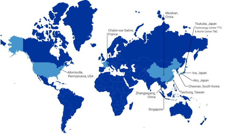
Our capabilities include 11 Electronics Materials Centers (EMCs) worldwide where Air Liquide produces, packages and certifies electronics specialty materials ensuring safety of supply and matching quality expectations of most demanding electronics customers. We are strategically located in electronics hubs including South Korea, Japan, China, Taiwan, Singapore, the USA, France and Germany.
With 30 years of experience in the electronics industry, we have unique expertise in the production of electronics specialty materials, as well as in stringent quality control, packaging and distribution under a strict corporate safety policy.